Active Rev A.1
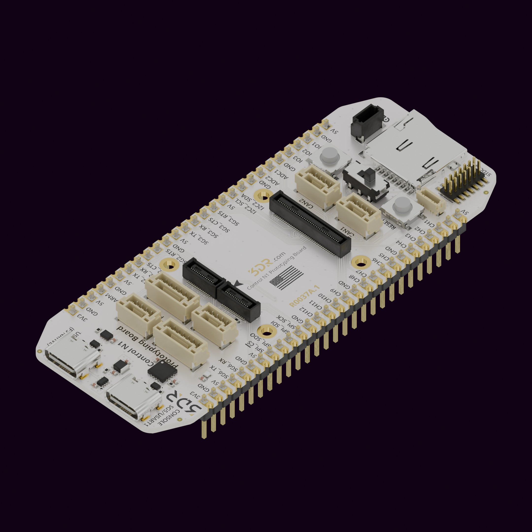
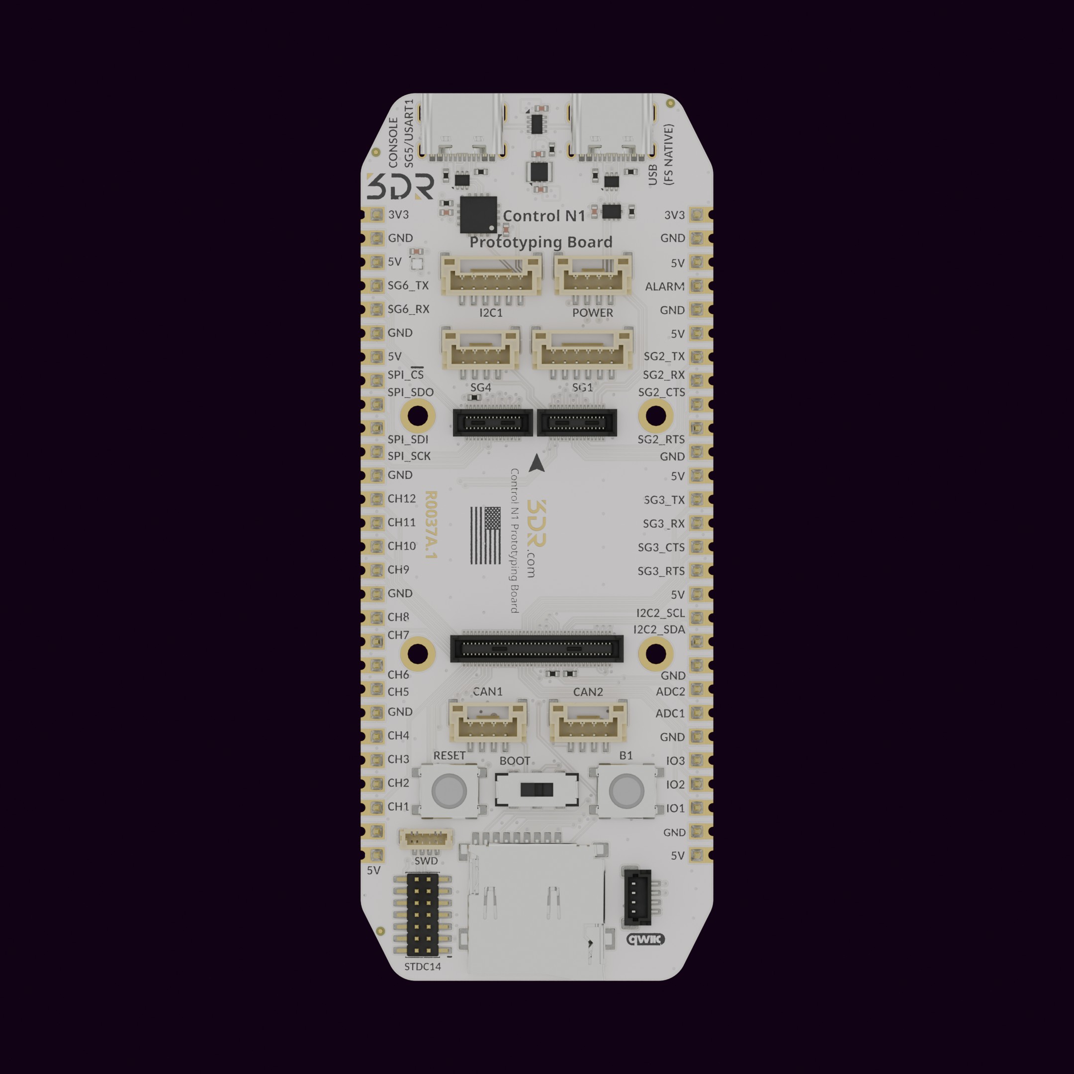
The R0037 is a prototyping carrier for the Control N1 , designed to accelerate hardware development without the constraints of a production carrier board. Standard pin spacing lets it seat directly into a breadboard for tool-free prototyping, with every pin on the CN1 broken out for direct access to all signals, plus two debug cable interfaces for programming. Use it to evaluate sensors and peripherals, probe CN1 signals, or test custom peripheral wiring before committing to a custom carrier board layout.
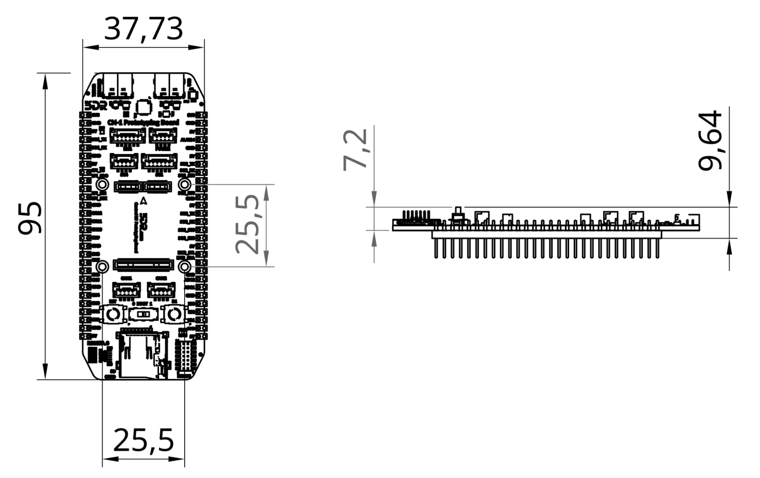
Specifications 3DR CN1 Prototyping Board (R0037) Mounting Holes M2 Weight 15g (without pin headers) Dimensions See Mechanical Information
Electrical Specifications 3DR CN1 Prototyping Board (R0037) Input Voltage 5V via USB 5V Output (Max Continuous) 1.5A (shared across 5V pads) 3.3V Output (Max Total) 600mA
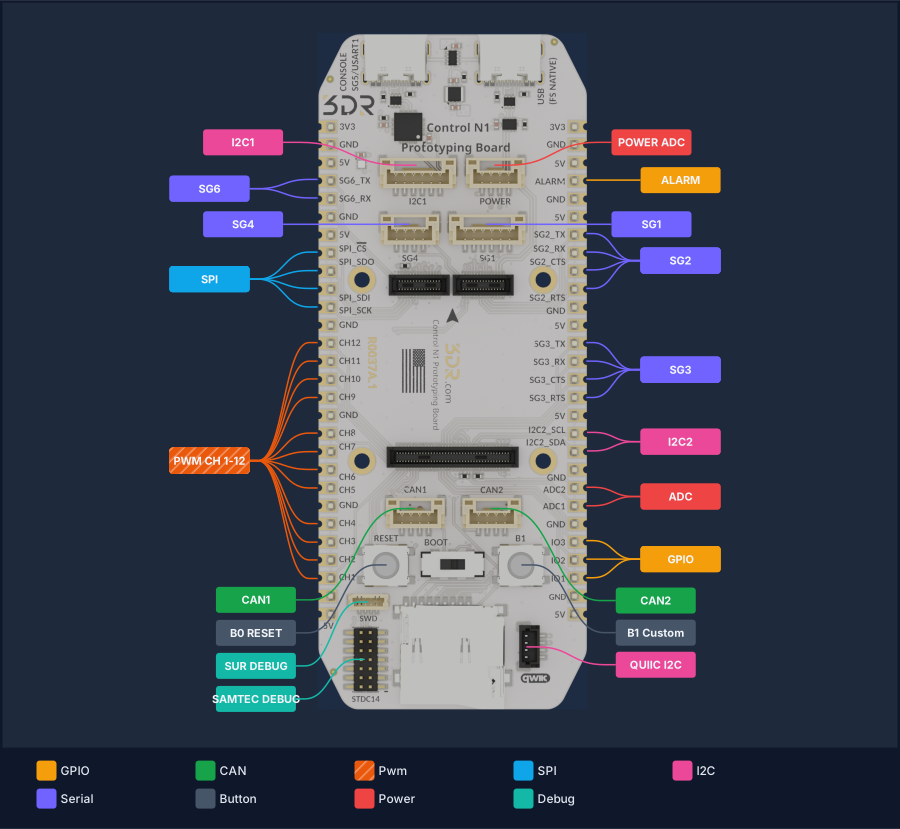
Port Connection Type USB-C (USB) USB-C USB-C (Console UART) USB-C Micro SD Card Slot Slot Boot Switch Switch RST (Push Button) Button B1 (Push Button) Button SG1 w/Flow Control Connector SG2 w/Flow Control Pads SG3 w/Flow Control Pads SG4 Connector SG5 Pads SG6 Pads PWM CH1–12 Pads GPIO 1–3 Pads I2C1 Connector I2C2 Pads SPI Pads CAN1 Connector CAN2 Connector Power Connector
Unpack the product and inspect for any visible damage. Align the connector/interface with the corresponding port on Control N1 (R0024) . Secure the connection by pressing firm and equally both boards against each other. Power On the base product to verify successful integration. Pin Signal Description 1 +5V +5V power output 2 S1_TX Serial transmit (UART TX) 3 S1_RX Serial receive (UART RX) 4 S1_CTS Clear To Send (hardware flow control) 5 S1_RTS Request To Send (hardware flow control) 6 GND Ground
Pin Signal Description 1 +5V +5V power output 2 S4_TX Serial transmit 3 S4_RX Serial receive 4 GND Ground
Pin Signal Description 1 +5V +5V power output 2 SCL I2C clock line 3 SDA I2C data line 4 GND Ground
Pin Signal Description 1 +5V +5V power output 2 CAN_H CAN bus high 3 CAN_L CAN bus low 4 GND Ground
Pin Signal Description 1 +5V +5V Power input 2 ADC2 Analog input 1 3 ADC1 Analog input 2 4 GND Ground
Button Pin Function RST AP_RST Resets the CN1 B1 IO4 User-assignable button
Position Function OFF Boot from internal flash (normal) ON Enter bootloader / DFU mode
All pads are labeled on the board itself.
USB 5V Rail (1.5A max) USB Console (FTDI → SG5) 3.3V Power Module (600mA max) 5V Pads Connectors Buttons 3V3 Pads Power Connector (Battery) 5V Rail (Battery) 3.3V Power Module (600mA max) 5V Pads Connectors Buttons 3V3 Pads Clean with a dry cloth; avoid moisture or abrasive materials. Periodically check connection points for wear or loosening. Store in a cool, dry place when not in use. If you have further questions, contact us .